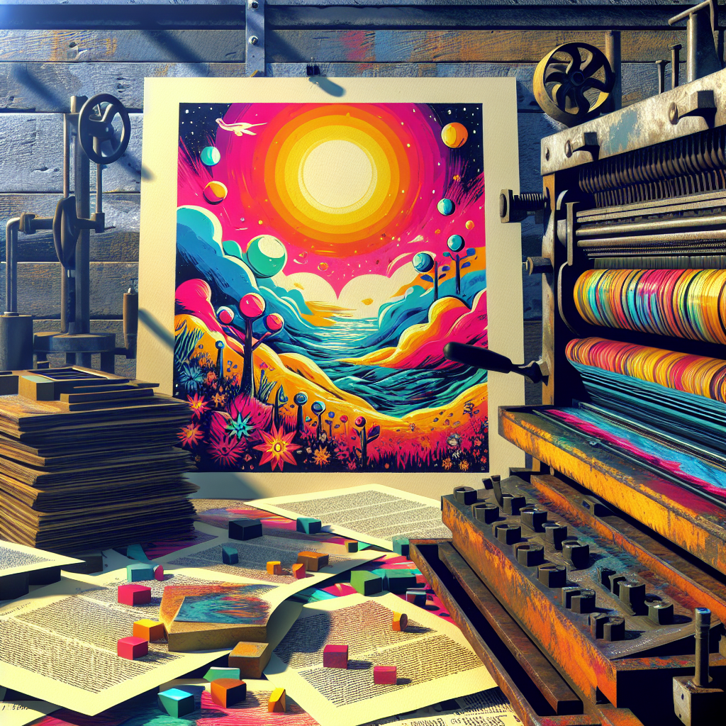
What is Lithography and Why is it So Fascinating?
Imagine a world where the tiniest details are etched with precision onto silicon chips, powering the very devices that shape our lives. Fascinating, right? This is the magic of lithography, a technology that underpins the modern advancements in computer chips and microelectronics. Stemming from the Greek words 'lithos' meaning 'stone' and 'graphia' meaning 'writing', lithography was invented in the late 18th century as a method of printing using stones. Fast forward to today, it’s become a cornerstone in the manufacturing of integrated circuits, making it essential to Gizmos and gadgets found across the globe.
The Evolution and Application of Lithography
Originally utilized by artists to produce prints, lithography has undergone several transformative adaptations throughout history. Alois Senefelder invented it in 1796 for artworks. But by the mid-20th century, this technique had migrated into the burgeoning field of semiconductor manufacturing. Here, lithography plays the role of a meticulous dance of light and chemistry, enabling the mass production of microchips. It's pivotal in driving progress in devices ranging from smartphones to supercomputers.
The most renowned type of lithography is photolithography, which uses light to transfer a geometric pattern from a photomask to a light-sensitive chemical photoresist on the substrate. Other methods such as electron-beam lithography, X-ray lithography, and extreme ultraviolet lithography (EUVL) also exist, each serving specific purposes and offering varied precision levels.
The Marvels of Photolithography in Electronics
Photolithography is the star of the show when it comes to the production of electronic goods. This process stands out due to its high precision and ability to create intricate patterns repeatedly. Essentially, it involves coating a silicon wafer with a light-sensitive photoresist, through which light shines, hardening the exposed regions. The unhardened areas are washed away, revealing a detailed pattern. This pattern is the blueprint that guides subsequent steps of etching and deposition to build circuits.
But what makes photolithography truly magical is its cyclical nature. Multiple layers can be stacked, each patterned meticulously, providing the complex, multi-functional architecture that defines modern processors. As electronics evolve and demand more functionality in smaller spaces, the capabilities of photolithography continue to push the boundaries of what was thought possible.
Extreme Ultraviolet Lithography: The New Frontier
Today, the forefront of lithography is Extreme Ultraviolet Lithography (EUVL). This advanced technique uses light with extremely short wavelengths to create incredibly small and precise geometry on the silicon wafer. The beauty of EUVL lies in its ability to print finer details with fewer steps, making it a more efficient and precise method.
However, like all great technological advances, EUVL presents its own set of challenges. The equipment required is incredibly complex and necessitates extreme precision and control over environmental conditions. Despite these challenges, EUVL is heralding a new era of even smaller and more powerful chips, promising an exciting future for technology.
The Far-Reaching Impact of Lithography
Why should we care so deeply about these intricate details of lithography? Well, it’s not just about computers getting faster or gadgets becoming more sophisticated. The principles of lithography foster innovation across a multitude of industries, from healthcare, with precise diagnostic equipment, to the automotive industry and even space exploration technologies.
Environmental concerns also come into play with advancements in lithography. As chip technologies become smaller and more energy-efficient, they contribute to more sustainable practices, promoting energy conservation across global electronic ecosystems. The ripple effects are considerable and underline the importance of advancing and refining lithographic techniques.
The Future Holds Limitless Potential
Looking ahead, the relentless drive to miniaturize and optimize suggests that lithography will continue to evolve, potentially incorporating even more radical methods. Explorations into beyond-lithography techniques, such as nanolithography or self-assembly processes, aim to alleviate current limitations and push the boundaries of what is possible even further.
What’s both thrilling and humbling about the field of lithography is how a technology rooted in ancient printing practices has become a pivotal player in modern scientific advancements. It embodies the essence of human creativity and ingenuity, consistently challenging the limits of what we can achieve.
Embracing Lithography’s Role in Our World
In this exciting journey of miniaturization and optimization, lithography serves not just as a testament to our technological prowess, but also as a reminder of the brilliant fusion of art and science. From its origins to its applications, it illustrates how our curiosity and determination to explore the unknown will continue to forge remarkable paths, lighting up the universe of possibilities.
In the captivating world of lithography, there is a key to unlocking the future, serving as a beacon of our persistent, optimistic pursuit of progress. It's an exhilarating time to witness these advancements and an even more thrilling prospect to imagine what's next.

