

Unboxing the Mystery: What is Flatpack Electronics?
Imagine a world where big, bulky electronic components seamlessly transform into small, sleek designs, almost like folding a beanbag into a pocket-sized cushion. Enter flatpack electronics! First developed by IBM in the 1960s, these ingenious devices have revolutionized the way we think about size, efficiency, and power in the world of electronics. Designed primarily to meet the need for compact and highly efficient packaging of components, flatpacks have become a foundational technology in fields like computing and telecommunications.
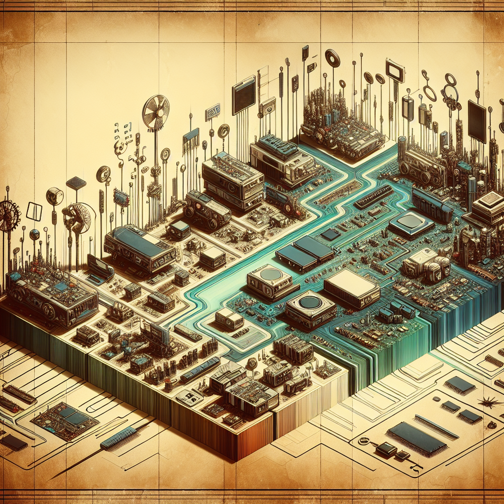
Flatpack electronics are a type of surface-mount technology that essentially "flattens" the packaging of electronic elements to save space. Instead of having components that protrude outwards like tiny skyscrapers on a circuit board, flatpacks lay everything flush, creating a neat, tidy landscape. This crucial advancement has allowed electronic devices to become ever smaller and more powerful, a trend we've seen accelerate with each generation of our favorite gadgets.
The Science Behind the Sleekness
So, how does this magic work? At the core of flatpack electronics is surface-mount technology (SMT), which differs fundamentally from the older through-hole technology (THT). In THT, you might recall that components have long metal leads or pins that are inserted through holes drilled in the circuit board. By contrast, SMT eliminates the need for these holes by mounting components directly onto the surface of the board.
Flatpack components are encapsulated in a flat, rectangular case with several pins on each side, allowing for maximum connectivity without unnecessary bulk. This configuration not only reduces the size of the components themselves but also minimizes the need for additional supporting structures, such as wiring or soldering materials, that make older designs cumbersome.
A Rewind Through Time: Flatpack's Evolution
Let's rewind the clock back to the early 1960s. The world was in the midst of a technological renaissance. IBM, always a pioneering force, needed a way to create more compact computers - devices that could revolutionize business, research, and personal use by freeing up space and presumably enabling greater portability. Thus, the flatpack was born. By the 1970s and 80s, the innovation had spread throughout the electronics industry, becoming a staple in consumer electronics.
Today, you'd be hard-pressed to find a circuit board that doesn't utilize this groundbreaking innovation in some capacity. In the evolutionary milestone of miniaturizing electronic components, flatpacks played a critical role, facilitating the dawn of portable consumer electronics such as laptops, mobile phones, and wearable devices.
Why Flatpack? The Expansive Impact
Ever wondered why we can carry supercomputers in our pockets these days? Flatpack electronics are a major reason why! The benefits they bring are multifold:
- Space-Saving Design: As devices reduce in size, the efficiency of flatpack contributes to a lighter, more compact end product.
- Enhanced Performance: Reduction in the component size and the proximity of elements can reduce latency and increase processing speeds.
- Cost Efficiency: By maximizing the utility of a circuit board's surface area, fewer materials are required, which in some cases, can lead to cost savings in production.
- Greater Durability: Fewer solder joints and connections mean there's less to break, increasing the overall reliability of the device.
Looking Ahead: The Future is Packaged Flat
The potential applications and advancements stemming from flatpack electronics excite scientists, engineers, and technophiles worldwide. They're not just central to today's achievements but also pivotal to the forward journey towards more advanced electronics. Imagine flexible electronics in wearables or highly efficient data centers that transform rapidly to meet demand.
As we venture further into a world fueled by the Internet of Things, smart cities, and AI, the demand for flatpack designed components will only grow. These components become more sophisticated each year, accommodating more complex functionalities while maintaining the streamlined, efficient design that flatpacks are famous for.
So the next time you pick up your smartphone or plug in your wearables for a jog, remember the flatpack electronic components inside that made it all possible. The extraordinary fusion of science and creativity continues to unfold, making our world smarter and interconnected!